555 IC Datasheet, Pinout, and Pins Function
555 Timer IC Functional Block Diagram
To understand how an adjustable delay timer relay module circuit works, you can carefully observe the functional block diagram and pin function descriptions of the 555 IC published below.
Pins Function of 555 Timer IC
To understand how the 555 IC delay timer circuit works, the pin assignment of the IC:
• Pin1 is the ground pin that connects to the negative (zero volts) power source.
• Pin2 is the Trigger pin. This pin enables the timing cycles for the circuit to operate. This pin is left free in the 555 IC delay timer circuit diagram because triggering is not required in this delay timer circuit.
• Pin3 is the Output pin. With a maximum current flow of 200mA, such a device can be loaded on this pin because the 555 timer IC can output a maximum current of two hundred milliamps.
• Pin4 is the Reset Pin. If the 555 IC needs to be reset in a particular circuit, connecting this reset pin to the ground will reset the IC's operation. This pin should be connected to the positive supply in a circuit that does not require resetting.
• Pin5 is the Control Voltage pin. This Control Voltage pin is connected to the inverting terminal of the internal comparator of the 555 IC; if an extra high or low voltage is required there, this threshold pin has to be supplied at that specified voltage.
• Pin6 is the Threshold pin. This threshold pin is connected to the non-inverting terminal of the internal comparator of the 555 IC. The output voltage/data is controlled by making this threshold pin voltage high or low compared to the internal inverting pin voltage.
•Pin7 is the discharge pin. This pin is connected to the collector of the IC's internal NPN transistor. When the base of this transistor is reverse-biased, its collector goes to low/0 voltage to discharge the time-determinant capacitor. This pin discharges a capacitor, and the timing of the 555 IC delay timer circuit depends on that discharge time.
•Pin8 is the VCC Pin. This pin needs a positive supply ranging from 3 volts to 15 volts. If the power source is not SMPS, a voltage regulator IC like 7805 or 7812 is better for making a 555 delay timer circuit.
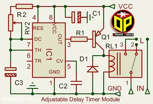
Delay Timer Schematic Circuit Diagram Using 555 IC
555 IC time delay circuit diagram is published below.
 |
555 IC Delay Timer Circuit Diagram |
Component List of 555 IC Adjustable Delay Timer Circuit Diagram
IC- NE555 IC or Equivalent
RL1- Use a 12-volt relay for a 12-volt circuit and a 5-volt relay for a 5-volt circuit.
D1- 1N4007
Q1- BC336 or A950 or Equivalent Silicon PNP Transistor.
C1- 470µF
C2- 0.1µF
C3- 330µF
R1- 10KΩ
R2- 4.7KΩ
RV2- 500KΩ Potentiometer.
555 IC Monostable Timer Calculation Formula:
In the monostable timing formula of the 555 IC, T is time, 1.1 is the RC constant, R is resistance, and C is capacitance. First, match the following formula with this information.
T = 1.1 x R x C
In this formula, R or resistance should be calculated using Ohm (Ω); if the resistance is 1KΩ, it will be 1000 Ohms. And C or Capacitance should be calculated in Farads (F), i.e., if the capacitance is 1µF, it will be 0.001F
Suppose you build a delay timer circuit for a refrigerator. In this case, the power supply to the refrigerator requires a 5-minute delay timer.
In this case, 5 minutes, 300 Seconds.
So, time in seconds (T) 300 = Constant 1.1 x 580,000Ω (580KΩ) x 0.47 Farad (470µF)
T = 1.1 x 580000Ω x 0.47F
Or 1.1 x 580000Ω x 0.47F = 299.86 Seconds or 5 Minutes.
Therefore, for a 5-minute delay timer, the R2 resistor (R2+RV2) value in the above circuit diagram will be 580KΩ, and the C1 capacitor value will be 470µF.
According to this formula for a 555 timer IC circuit, you can make a delay timer circuit from a microsecond to a few hours.
555 IC: What are astable and monostable circuits, and what are their differences?
A 555 IC delay timer is a monostable circuit that turns on for a specified time. Here is an example of a stable circuit of a 555 timer IC, which turns off and on continuously according to a specified time.


No comments:
Post a Comment