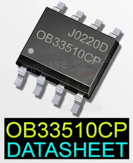
The OB33510CP IC is a highly integrated PWM controller specifically designed for LED backlight applications in modern LCD TVs and monitors. This 8-pin SMD IC stands out because it requires very few external components, making it an ideal choice for compact LED driver boards where space and cost-efficiency are crucial.
One of the most important features of the 0B33510CP IC is its built-in safety mechanism, which includes Over Voltage Protection (OVP) and Thermal Shutdown. These features ensure that the backlight LEDs remain protected even during voltage fluctuations or overheating, significantly extending the lifespan of the display panel.
OB33510CP IC or 0B33510CP IC Schematic Circuit Diagram Datasheet (Pinout). Application- LED Driver of LCD TV / LCD Monitor. OB33510CP IC is mainly used in LED driver circuits. LED TV, LCD TVs, and flat panel displays have this LED driver circuit. A pulse width module (PWM) or analog dimming mode is available in the OB33510CP IC.
The OB33510CP IC has a built-in 100-volt power MOSFET for amplifying weak pulses. The operating voltage or input voltage range of the OB33510CP IC is 9 volts to 30 volts. This 8-pin OB33510CP SMD IC is widely used in LED LCD TV combo boards because the performance of the OB33510CP IC is excellent.
OB33510CP Schematic Circuit Diagram With Pinout Data

|
|
OB33510CP IC Schematic Circuit Diagram |
OB33510CP IC Pinout and Pins Function
How to make VGH VGL AVDD VCOM Module Using NE555 IC?
- PIN 1 - OVP (Over Voltage Protection): This part of the IC monitors the current flowing through the LED through R2 and R3. If the VIN voltage rises beyond the threshold, the OVP circuit activates and resets the PWM signal to protect the LEDs.
- PIN 2 - PWM (Pulse Width Modulation): Controls the brightness of the LED TV's backlight. This pin is governed by the processor IC of the LED TV.
- PIN 3 - VIN (Voltage Input): Power supply pin where 9V to 30V is applied.
- PIN 4 - Drain: Connected to the internal 100V MOSFET drain terminal. It outputs the voltage for the backlight LED through the converter inductor.
- PIN 5 - CS (Current Sense): Connected to the current sense amplifier and ramp adjustment circuit for stable operation.
- PIN 6 - GND: System ground pin.
- PIN 7 - FB (Feedback): Feedback pin to control and stabilize the output voltage based on LED current.
- PIN 8 - COMP (Compensation): Boost converter loop compensation terminal to control current based on the load.
Sony Bravia Smart TV Red Light Blinking 2 Times? Click Here

|
OB33510CP IC / 0B33510CP IC Pinout Connection |
So far, I am still looking for an IC compatible with the OB33510CP IC in any LED TV or monitor; if I find any substitute IC for the OB33510CP IC in any LED TV board, I will update that information here.
SM4186 T-Con with DC to DC Converter IC Data - CLICK HERE
Practical Video Guide: OB33510CP IC Backlight Repair
If you want to understand how the OB33510CP IC functions in a real circuit, this practical repair video is for you. In this video, I have demonstrated the step-by-step troubleshooting process for LED TV backlight issues, including voltage measurements and the protection mode logic. Watch the full video below to enhance your technical skills and master the art of LED driver repair.


2 comments:
আমি কি আপনার মোবাইল নাম্বারটি পেতে পারি , আমার একটি ৪২ ইন্চি নন ব্রান্ড স্ম্রাট টিভি আছে , ছবি আসেনা কথা আসে ।
Very usefull information about BL Driver.
Post a Comment