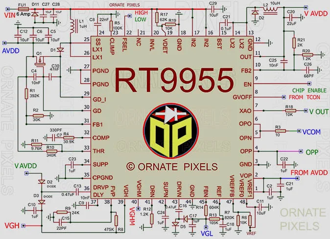
RT9955 IC Schematic Circuit Diagram, Substitute or Equivalent, Datasheet, and Pinout:
The RT9955 IC has a buck converter with a boost regulator to provide the required voltage to all thin-film transistors (TFT) placed on the liquid crystal display panel used in LCD TVs/monitors.
The RT9955 IC has a 20V 3Amp 0.15 ohm N Channel internal MOSFET to output the voltages from the boost regulator and buck converter circuits. An adjustable charge pump regulator circuit is implemented in converter circuits and in the RT9955 IC for high gate voltage (VGH) and Low Gate Voltage (VGL) outputs for the TFT gate driver for the LCD Panel.
The RT9955 IC has programable automatic over-voltage, under-voltage,
over-temperature, and over-current control and protection circuits. The standard voltage (VCOM) output is regulated by an internal operational amplifier (OPAMP) in the RT9955 IC to properly control the image contrast of the LCD TV or monitor.
The operating voltage (VIN) of the RT995 IC is 8 to 14 volts DC. This IC has a voltage detector circuit XAO that monitors and resets the signal when the VIN voltage drops.
Here are all LED TV Service Menu Codes
RT9955 IC Schematic Circuit Diagram Pinout and Substitute
 |
| RT9955 IC Schematic Circuit Diagram and Pinout |
Pin No - PIN NAME - PIN FUNCTION of RT9955 IC
1 - 1 VREFI - Voltage Reference_I, Internal Linear regulator input terminal
2 - VOP - Supply input for Operational Amplifier
3 - OGND - Operational Amplifier ground
4 - OPP - (Internal OPAMP) Operational Amplifier non-inverting input
5 - OPN - The inverting input of the Internal Operational Amplifier
6 - OPO - The output of the operational amplifier (Internal OPAMP Circuit of RT9955 IC )
7 - XAO - Voltage detector for reset function
8 - GVOFF - Switching input terminal from TCON for high voltage control.
9 - EN - Enable VGH charge pump
10 - FB2 - Feedback voltage input terminal from the buck regulator output
11 - OUT - The output sense input terminal of the buck converter
12 - GND - The ground of the bulk regulator output section
13,14 - LX2 - The source terminal of the internal MOSFET of the buck regulator output
15 - BST - Bootstrap is the Internal Supply terminal of the side MOSFET gate driver
16,17 - IN2 - Input, Supply voltage input (Operating voltage)
18 - GND - The ground of the VGL charge pump
19 - VDET - Voltage detection input terminal
20 - INVL - Supply voltage terminal of internal 4-volt regulator circuit of RT9955 IC
21 - NC - Not Connected
22 - FSEL - Frequency Selection Terminal of High or Low frequency (750Khz and 500Khz)
23 - CLIM - Over-current protection setting terminal
24 - SS - Soft Start terminal
25,26 - LX1 - The source terminal of internal MOSFET
27,28 -. PGND - Power ground of boost regulator
29 - GD I - Output sense terminal for over-voltage trucking
30 - GD - Gate Driver Terminal of MOSFET for AVDD output
31 - FB - Feedback terminal for output voltage and frequency control
32 - COMP - Compensation terminal of boost regulator error amplifier
33 - THR - Adjustment input for VGHM falling regulation
34 - SUPP - Supply terminal of VGH charge pump regulator (internal circuit of RT9955 IC)
35 - CPGND - Charge Pump Ground circuit
36 - DRVP - Driver output of VGH charge pump regulator
37 - DLY1 - Delay
38 - FBP VGH Feedback pulse input terminal (internal)
39 - VGH - VGH
40 - VGHM - VGHM
41 - DRN - GPM Discharge terminal
42 - SUPN Internal regulator supply input terminal of VGL charge pump circuit
43 - DRVN The output pin of VGL
44 - GND The ground of the VGL charge pump
45 - FBN VGL Feedback
46 - REF Reference output ( Follow- RT9955 IC Schematic circuit diagram )
47 - VREF_FB Feedback input of the linear regulator
48 - The linear regulator output terminal
(Solution For Sony Bravia TV Red Light Blinking 2-Times? )
Substitute or the equivalent of RT9955 IC
I found another 48-pin IC circuit that is identical to the RT9955 IC circuit. That IC can be a Substitute for the RT9955 IC. I will give you the next post very soon after I make sure.(Please download and zoom the image to see the serial numbers of the small components in the RT9955 circuit diagram)
More IC Datasheet- SM4186 IC Datasheet


No comments:
Post a Comment